Solution Overview
This granite/marble lithography machine base is specifically designed for semiconductor lithography equipment (DUV Deep Ultraviolet Lithography Machines, EUV Extreme Ultraviolet Lithography Machines). With “nano-level reference precision, full-scenario anti-interference, and in-depth integration with lithography systems” as its core, it addresses three key pain points of traditional metal bases: “precision drift caused by thermal deformation, vibration interference with lithography positioning, and precision degradation after long-term use”.
Leveraging the ultra-low thermal expansion coefficient, superior vibration resistance, and non-magnetic properties of high-density natural stone, it provides a stable reference carrier for lithography in advanced processes of 5nm and below. It ensures the positioning accuracy of the lithography machine’s wafer stage is ≤ ±0.5nm and the lithography overlay accuracy is ≤ ±1nm, helping to increase the yield of semiconductor chip manufacturing by 3%-5%. This meets the strict requirements for equipment references in advanced process production lines of manufacturers such as TSMC and SMIC.
Core Function System
1. Nano-Level Reference Precision Guarantee
- Extreme Flatness and Straightness: High-density granite is selected and processed through a three-stage process of “rough grinding – fine grinding – nano-level polishing”. The flatness of the base’s top surface is ≤ 0.001mm per 1000mm (for single-piece bases) and ≤ 0.002mm per 2000mm (for spliced bases); the straightness of the guideway installation reference surface is ≤ 0.0008mm per 1000mm, and the surface roughness is Ra ≤ 0.01μm. This provides nano-level reference support for the wafer stage and projection lens, avoiding lithography pattern offset caused by reference deviations.
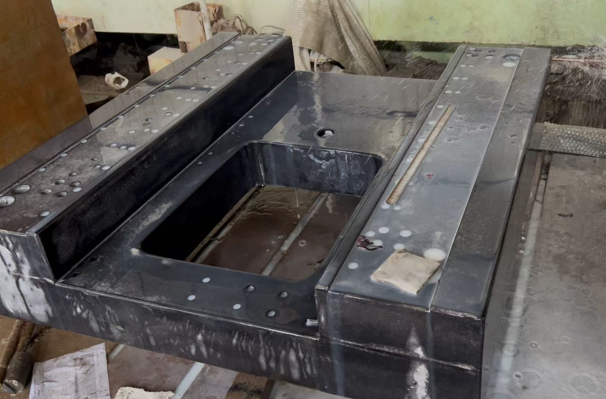
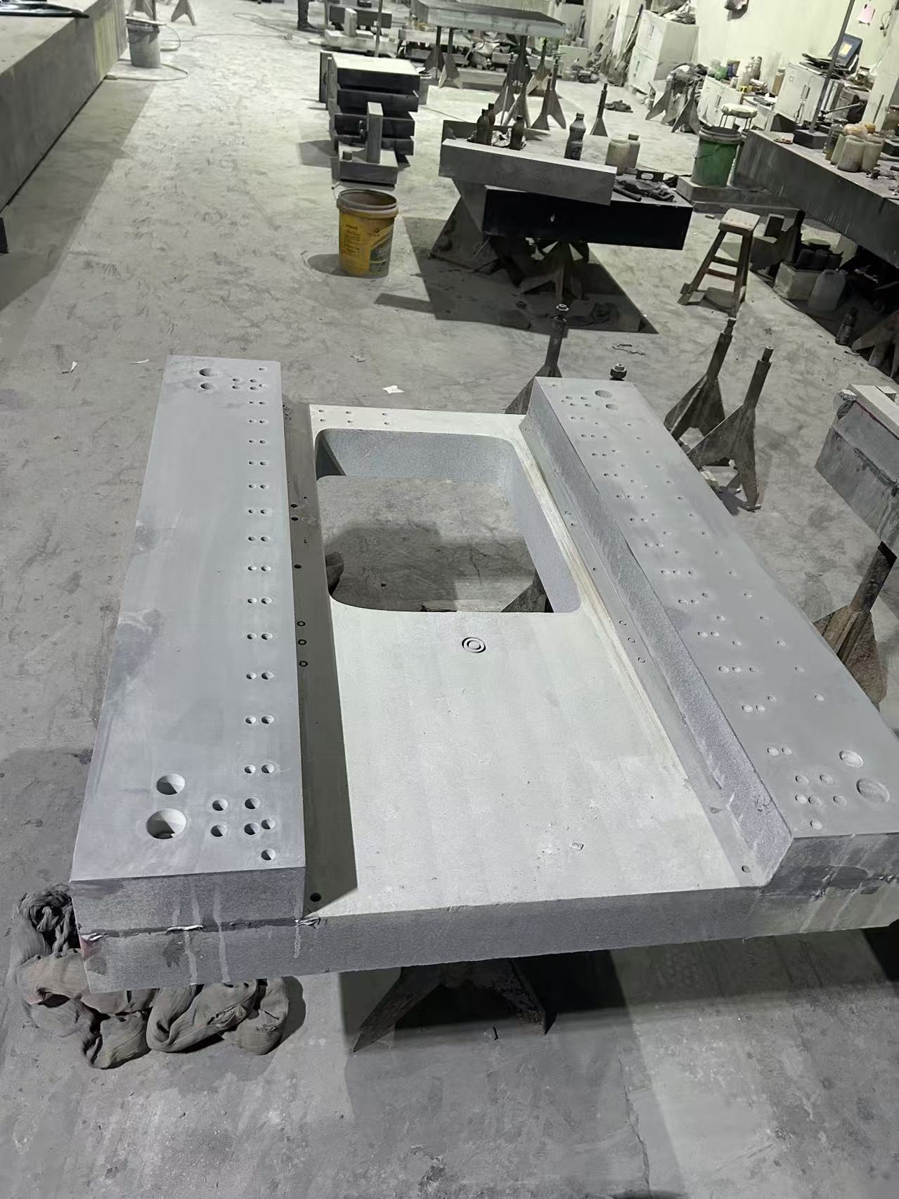
- Ultra-Low Stress Stable Structure: After 36 months of natural aging (twice the duration of ordinary mechanical components) + 2 rounds of artificial aging treatment, more than 99.5% of internal stress is eliminated. An “integral casting + non-splicing” structure is adopted (maximum single-piece size: 4000×2500mm) to avoid precision steps caused by splicing seams. Under long-term load (wafer stage + wafer weight: approximately 500kg), the deformation is ≤ 0.0005mm per meter, ensuring no micro-deformation of the reference during lithography.
- Nano-Level Positioning Reference Integration: Precision mounting reference holes (φ10-φ20mm, tolerance H6) and positioning pin holes (hole position tolerance ±0.002mm) for the wafer stage are machined on the base surface. Combined with laser interferometer calibration, the positioning deviation between the wafer stage and the base is ≤ ±0.1nm, providing a fundamental guarantee for lithography overlay accuracy.
2. Full-Scenario Anti-Interference Stable Control
- Thermostatic Thermal Deformation Suppression: The thermal expansion coefficient of natural granite is as low as (5-6)×10⁻⁶ per ℃ (20% lower than ordinary granite). A high-precision constant-temperature water circuit (aperture φ8-φ12mm, water circuit spacing 200mm) is integrated inside the base. Cooperating with the constant-temperature system of the semiconductor cleanroom, the overall temperature uniformity of the base is ≤ ±0.1℃, and the dimensional change caused by temperature fluctuation is ≤ 0.0001mm per meter. This avoids the impact of thermal deformation on the relative position between the wafer stage and the projection lens.
- Full-Range Isolation of Micro-Vibrations: The internal damping coefficient of stone is 5-8 times that of cast iron, with a vibration attenuation rate of ≥ 90% (80% for ordinary granite), which can absorb high-frequency micro-vibrations (10-1000Hz) generated inside the lithography machine (e.g., vacuum pumps, motors). The bottom of the base is equipped with an air spring vibration damping system (vibration damping efficiency ≥ 95%) to isolate low-frequency vibrations (1-10Hz) from external equipment in the cleanroom (e.g., robotic arms, conveyor belts). This ensures the vibration amplitude of the wafer stage during lithography is ≤ ±0.3nm.
- Non-Magnetic and Chemical Corrosion Resistance: Natural granite/marble is non-magnetic, avoiding magnetic field interference with electron beam focusing in EUV lithography machines or laser transmission in DUV lithography machines. The surface is treated with a “nano-level ceramic coating” (thickness 5-10μm), which is resistant to common semiconductor chemical reagents such as photoresist, isopropyl alcohol, and developer. It is free from corrosion and residue, and the surface finish does not degrade after long-term use.
3. In-Depth Integration Adaptation for Lithography Systems
- Collaborative Installation of Multi-Core Components: The base reserves dedicated installation areas for the wafer stage, projection lens, and light source system. The parallelism of the reference surfaces in each area is ≤ 0.001mm per 1500mm. Precision threaded holes (M8-M16, thread tolerance 5g) and vacuum suction interfaces (φ6-φ10mm) are machined to adapt to the vacuum fixation and high-precision drive system of the wafer stage, reducing positioning errors caused by intermediate connectors.
- Cable and Optical Path Compatibility Design: Concealed cable channels (aperture φ15-φ25mm) and optical path avoidance grooves (width 10-20mm, depth 5-10mm) are opened inside the base. This prevents the lithography optical path from being blocked by the base structure and avoids cable pulling affecting the motion accuracy of the wafer stage. The inner walls of the channels are smoothed to reduce air disturbance (micro-airflow control is required in semiconductor cleanrooms).
- Reserved Detection and Calibration Interfaces: Laser interferometer calibration reference points (interval 500mm, accuracy ±0.0005mm) and temperature sensor mounting holes (φ3-φ5mm) are reserved. This facilitates regular detection and calibration of base precision and temperature distribution without disassembling the core lithography components, improving calibration efficiency by 80%.
Core System Composition
| Component Category |
Core Parameters and Configuration (Semiconductor Lithography-Specific) |
| Base Body (Granite) |
Material: High-density Jinan Green Granite (density ≥ 2.7g/cm³, water absorption rate ≤ 0.05%, impurity content ≤ 0.1%); Precision: Top surface flatness ≤ 0.001mm per 1000mm, guideway reference surface straightness ≤ 0.0008mm per 1000mm, surface roughness Ra ≤ 0.01μm; Dimensions: Standard single-piece 1500×1200mm~4000×2500mm, maximum spliced size 6000×3000mm; Processing Technology: 36-month natural aging + nano-level polishing + nano-ceramic coating (chemical corrosion resistance) |
| Base Body (Marble) |
Material: High-purity black marble (calcium carbonate content ≥ 99%, density ≥ 2.75g/cm³); Precision: Top surface flatness ≤ 0.002mm per 1000mm, surface roughness Ra ≤ 0.02μm; Application Scenarios: DUV lithography machines (14nm and above processes), load-bearing capacity ≤ 300kg/m² |
| Anti-Interference Components |
Constant-temperature water circuit (aperture φ8-φ12mm, temperature control accuracy ±0.1℃); Air spring vibration damping modules (vibration damping efficiency ≥ 95%, adaptable to 1-1000Hz vibrations); Non-magnetic gaskets (to avoid magnetic field interference) |
| Integration-Adaptation Components |
Wafer stage mounting reference holes (φ10-φ20mm, tolerance H6, hole position tolerance ±0.002mm); Vacuum suction interfaces (φ6-φ10mm, vacuum degree ≤ -95kPa); Laser calibration reference points (accuracy ±0.0005mm); Concealed cable channels (aperture φ15-φ25mm) |
Typical Industry Application Cases
- 5nm EUV Lithography Machine Base: A semiconductor equipment manufacturer uses it for a 5nm EUV lithography machine (wafer stage stroke 800mm) — a single-piece Jinan Green Granite base (3000×2000×600mm) is adopted, with a flatness of ≤ 0.001mm per 2000mm. Cooperating with the constant-temperature water circuit and air spring vibration damping, the wafer stage positioning accuracy is improved from ±1nm to ±0.5nm, the lithography overlay error is ≤ ±0.8nm, and the 5nm chip yield is increased by 4.2%.
- 14nm DUV Lithography Machine Base: A wafer foundry uses it for the upgrade of a 14nm DUV lithography machine — the original metal base is replaced with a black marble base (2500×1800×500mm). The thermal deformation is reduced from 0.002mm per meter to 0.0005mm per meter, the vibration amplitude is reduced from ±2nm to ±0.8nm, the maintenance cycle of the lithography machine is extended from 3 months to 6 months, and the operation and maintenance cost is reduced by 35%.
- Advanced Packaging Lithography Base: A packaging and testing enterprise uses it for 2.5D/3D advanced packaging lithography equipment — a custom spliced granite base (4000×2500mm) is adopted to adapt to multi-station lithography needs. The parallelism of the reference surfaces of each station is ≤ 0.002mm per 3000mm, and the packaging yield is increased from 96% to 98.5%.
Core Competitive Advantages
- Nano-Level Precision Barrier: The flatness and straightness indicators far exceed those of ordinary mechanical components (one order of magnitude higher than Grade 00 precision), adapting to lithography in advanced processes of 5nm and below. It is the only alternative to metal bases (which cannot achieve long-term nano-level precision).
- Full-Dimensional Anti-Interference Capability: Exclusive optimization is made for the four major interference sources in semiconductor lithography (temperature, vibration, magnetic field, chemical corrosion). The vibration attenuation rate is 10% higher than that of ordinary granite components, and the temperature control accuracy is doubled, ensuring “zero interference” during the lithography process.
- Long-Term Precision Stability: After 36 months of natural aging + nano-coating protection, the precision retention period is more than 5 years (only 1-2 years for metal bases). This reduces the downtime of the lithography machine due to frequent calibration, saving wafer fabs more than 200 hours of downtime losses annually.
- Exclusive Integration for Lithography Systems: The reserved mounting references, water circuits, and interfaces are fully compatible with the core components of lithography machines (wafer stage, projection lens). The integration and commissioning time is shortened from 15 days (for traditional metal bases) to 5 days, reducing the integration cost of equipment manufacturers.
Full-Dimensional Customization Services
- Process-Specific Customization:
◦ Advanced Process Nodes (5nm and below): Custom high-density Jinan Green Granite bases with nano-level polishing + constant-temperature water circuits, and precision enhanced to flatness ≤ 0.0008mm per 1000mm;
◦ Mature Process Nodes (14nm-90nm): Black marble bases are optional to balance precision and cost, with flatness ≤ 0.002mm per 1000mm.
- Structure and Integration Customization:
◦ Dimension Customization: Single-piece or spliced structure, maximum support for 6000×3000mm, thickness 500-800mm (based on load requirements);
◦ Interface Customization: Custom mounting holes, vacuum interfaces, and cable channels according to lithography machine models (e.g., ASML, Nikon, Canon) to achieve “plug-and-play”.
- Precision and Detection Customization:
◦ Precision Enhancement: Local nano-level polishing is performed on key areas (e.g., projection lens mounting surfaces), with surface roughness Ra ≤ 0.008μm;
◦ Detection Services: Provide third-party nano-level precision detection (e.g., German Zeiss laser interferometer) and issue detection reports recognized by the semiconductor industry.
- After-Sales and Operation & Maintenance Customization:
◦ Installation and Commissioning: On-site nano-level horizontal calibration (accuracy ≤ 0.0005mm per meter) and collaborative commissioning with the lithography machine’s wafer stage and vibration damping system;
◦ Long-Term Operation & Maintenance: Customize a “1-year precision calibration + 3-year surface maintenance” plan, with lifelong technical support to ensure the base precision meets lithography requirements for a long time.